


Silicon wafers are the essential building blocks of nearly all modern electronics. They serve as the substrate on which electronic circuits are built, making them the foundation for semiconductors, integrated circuits (ICs), and microchips that power everything from smartphones to supercomputers, medical devices, and solar panels. The development and refinement of silicon wafers have been key to the rapid advancement of technology, enabling smaller, faster, and more powerful electronic devices.
In this article, we will explore the role of silicon wafers in electronics, their importance in semiconductor manufacturing, and how they enable the functionality of the electronic devices we rely on daily.
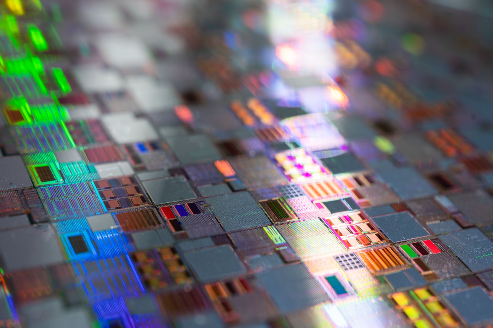
What is a Silicon Wafer?
A silicon wafer is a thin, flat disc made from highly purified crystalline silicon. These wafers are produced through a complex process of silicon purification, crystal growth, and wafer slicing, followed by polishing to create a smooth surface. Silicon wafers typically range in size from 100 mm to 300 mm (4 to 12 inches) in diameter, though larger wafers are also produced for specialized applications.
The primary role of the silicon wafer is to act as a substrate or base material for semiconductor devices. A wide variety of electronic components, such as transistors, capacitors, and diodes, are fabricated onto the surface of the silicon wafer through a series of processes that include doping, etching, and deposition. These components form the integrated circuits that enable electronic devices to perform complex tasks.
Why Silicon? Understanding Its Importance in Electronics
Silicon is the material of choice for electronic components due to its semiconducting properties. As a semiconductor, silicon can conduct electricity under certain conditions but also act as an insulator in others. This property allows engineers to precisely control the flow of electricity through a silicon wafer, making it ideal for building transistors and other components.
Key Properties of Silicon:
- Semiconductivity: Silicon can be doped with impurities like boron or phosphorus to control its electrical properties, allowing for the creation of p-type and n-type regions. This is crucial for forming transistors, the basic building blocks of all electronic devices.
- Abundance and Cost-Effectiveness: Silicon is the second most abundant element in the Earth’s crust, making it relatively inexpensive and widely available for mass production of electronics.
- Thermal Stability: Silicon is highly stable at the temperatures typically used in semiconductor manufacturing, making it suitable for high-performance electronics.
- Crystal Structure: Silicon can be grown into single-crystal structures with high purity, which is necessary for the precise fabrication of electronic circuits.
The Role of Silicon Wafers in Semiconductor Devices
The primary role of silicon wafers is to serve as the substrate for semiconductor devices. These devices are critical for controlling the flow of electrical current in circuits. The two main categories of semiconductor devices are discrete components (such as diodes and transistors) and integrated circuits (ICs), which contain millions or even billions of components on a single chip.
1. Transistors: The Building Blocks of Modern Electronics
Transistors are perhaps the most important components in modern electronics, acting as switches or amplifiers that regulate electrical signals. Silicon wafers are used to fabricate millions of transistors on a single chip. Each transistor is made by doping specific regions of the silicon wafer to create p-n junctions, which allow the transistor to control the flow of electrons through the circuit.
The miniaturization of transistors, driven by advancements in silicon wafer processing, has led to the exponential growth in computing power described by Moore’s Law—the observation that the number of transistors on a chip doubles approximately every two years.
2. Integrated Circuits (ICs): The Core of Microchips
Integrated circuits are formed by combining millions of transistors and other components onto a single silicon wafer. These ICs are the “brains” of all modern electronic devices, enabling functions like data processing, memory storage, and power management. Without silicon wafers, it would be impossible to create the densely packed circuits required for modern computing.
Some common examples of ICs include:
- Microprocessors: The central processing unit (CPU) of a computer or smartphone, responsible for executing instructions and performing calculations.
- Memory Chips: Used in devices like RAM (random access memory) and flash memory, which store data and allow for fast retrieval.
- Digital Signal Processors (DSPs): Specialized ICs used for processing audio, video, and other real-time data.
3. Photovoltaic Cells: Silicon Wafers in Solar Energy
Silicon wafers are not only essential for semiconductors but also play a critical role in renewable energy technologies, particularly solar panels. In photovoltaic (PV) cells, silicon wafers serve as the base material for converting sunlight into electrical energy. When sunlight hits the silicon wafer, it excites electrons, generating an electric current that can be harvested and used as power.
The same semiconducting properties that make silicon ideal for electronics also make it perfect for solar energy generation. Silicon-based PV cells are the most widely used type of solar cell due to their efficiency and cost-effectiveness.
Silicon Wafer Processing: From Raw Silicon to Functional Microchip
The role of silicon wafers in electronics is fully realized through the semiconductor fabrication process, which consists of several key steps designed to create functional electronic devices on the wafer surface.
- Wafer Fabrication: The process starts with purifying silicon and growing it into a single crystal using the Czochralski (CZ) method. This crystal is then sliced into thin wafers, which are polished to achieve a smooth and defect-free surface. The wafers must be perfectly flat, as any surface irregularities can lead to defects in the circuits that are later built on them.
- Photolithography: Photolithography is used to transfer circuit patterns onto the silicon wafer. A light-sensitive material called photoresist is applied to the wafer, and UV light is used to expose the desired pattern onto the surface. This pattern represents the layout of the transistors and other components that will be fabricated onto the wafer.
- Etching and Doping: Once the circuit pattern is created, etching is used to remove material from specific areas of the wafer, shaping the components. In the doping process, impurities like boron or phosphorus are introduced into the silicon to create regions with different electrical properties. This step is essential for forming the transistors, capacitors, and resistors that make up the microchip.
- 4. Deposition and Metallization: Thin layers of material, such as silicon dioxide or metal, are deposited onto the wafer through techniques like chemical vapor deposition (CVD) or physical vapor deposition (PVD). These layers form the insulation and wiring necessary for the components to function. Metallization involves adding conductive paths made of materials like aluminium or copper to connect the transistors and other components.
- 5. Testing and Packaging: After the electronic components are fabricated on the wafer, the wafer is cut into individual dies, each representing a microchip. These chips undergo testing to ensure they meet performance standards. Once tested, the chips are packaged into protective casings and prepared for integration into electronic devices.
Applications of Silicon Wafers in Modern Electronics
Silicon wafers are used in virtually all electronic devices, from consumer electronics to industrial and automotive applications. Here are some of the primary areas where silicon wafers play a critical role:
- Computers and Smartphones: Central processing units (CPUs), memory chips, and GPUs (graphics processing units) in these devices are all made using silicon wafers.
- Medical Devices: Silicon wafers are used to create components for diagnostic devices, pacemakers, and other medical equipment that requires precise control of electrical signals.
- Automotive Industry: Modern vehicles rely on silicon-based semiconductors for engine control units, safety systems, and infotainment features.
- Telecommunications: Integrated circuits made from silicon wafers are essential for devices such as mobile phones, routers, and network infrastructure equipment.
- Renewable Energy: Silicon wafers are used in the photovoltaic cells of solar panels, helping convert sunlight into clean energy.
Silicon wafers play a pivotal role in the modern electronics industry, providing the foundation for nearly every semiconductor device. Whether used in microchips, processors, memory modules, or solar cells, silicon wafers are at the heart of the technological revolution that has shaped our world over the last few decades.
By enabling the mass production of small, powerful, and energy-efficient devices, silicon wafers have driven advancements in computing, telecommunications, healthcare, and renewable energy. As technology continues to evolve, innovations in silicon wafer processing will remain crucial to the development of faster, smaller, and more efficient electronic devices.


